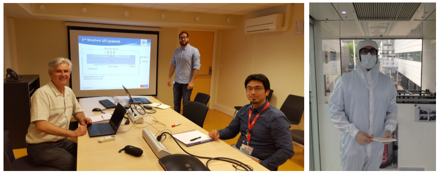
CAPPA PhD student Simone Iadanza recently visited CEA-Leti for a two-day period. Simone had a successful proposal funded by ASCENT. Through the ASCENT framework he received funding for processing some polycrystalline silicon wafers in CEA-Leti through their standard deposition – anneal – chemical – mechanical polishing, he is continuing this process as part of the DANCeR project. During his visit Simone gave a presentation on the work he had conducted to date on the first batch of wafers, had a detailed meeting with senior engineers who carried out the work on the batch of wafers in order to get details on the fabrication and parameters and data. He had several discussions about his current results and the continuation of the work, with a specific focus on how to tailor the fabrication processes for specific targets on a new batch of wafers. Simone also had a visit to some of the cleanrooms with information on process feasibility and their technical capabilities and he also visited the characterization labs.
As part of the DANCeR project, the nanophotonic group at CAPPA is developing a new framework for optical links, even as far as global on-chip interconnects. The project is based on the efficient coupling of the Photonic Crystal resonators with the outside world. These provide the ultimate confinement of light in both space and time allowing orders of magnitude improvements in performance relative to the state of the art, yet simpler system. New versions of the key components of optical links – light sources, modulators and photon-detectors – will be realised in this new framework providing a new paradigm for energy efficient communication.


