Materials
Experimental and theoretical work carried out by many leading physicists, including Albert Einstein, at the beginning of the 20th century, changed the way we understand the nature of light. It was shown that light consists of a fundamental particle, called a photon, which can be seen as a packet of light or radiation. While light is commonly associated with the visible colours seen in everyday life, it consists of a wide range of frequencies divided into different regions, for example, X-ray radiation, Ultraviolet radiation, Visible light and Infrared radiation, all part of the electromagnetic spectrum. The various regions of the electromagnetic spectrum will interact with matter in significantly different ways. The main interaction of light with matter consists of, energetic ejection or excitation of core electrons, excitation of molecular and atomic valence electrons, molecular electron excitation, molecular vibration or rotation. The outcome of these interactions with matter leads to transmission, reflection or an absorption process that may lead to a re-emission of light. For example, the interaction of visible light and leaves on vegetation leads to both a reflection (typically a green colour) and absorption due to chlorophyll, a common molecule found in plants. By using these interactions of light and matter, it is possible to probe the atomic and molecular structure of matter and falls within the field of spectroscopy.
Nano Diamonds
Nanodiamonds or diamond nanoparticles, are diamonds with a size below 1 micrometre. They can be produced by impact events such as an explosion or meteoritic impacts. Because of their inexpensive, large-scale synthesis, potential for surface functionalization, and high biocompatibility, nanodiamonds are widely investigated as a potential material in biological and electronic applications and quantum engineering.
Ideal diamond is a wide band-gap semiconductor with indirect energy gap of 5.45 eV and direct gap at Γ point of 7.3 eV at room temperature. Deep UV excitation assures excitation of not only ground electronic state but also all defect- and impurity-related bands and sub-bands present inside the band-gap. In an indirect gap crystal (Si, Ge, diamond…) the radiative recombination of photo-excited electrons from conduction band to valence band by means of light emission is a process of extremely low probability. The most probable scenario in an optically-excited crystal is a cascade of phonon-related non-radiative recombination events, combined with an excitation of optically-active impurities or defects levels (usually visible and IR fluorescence). The most common impurity levels and bands in diamond are nitrogen donor (1.7 eV), boron acceptor (0.37 eV), phosphorous donor (0.6 eV), and Sulphur donor (0.39-0.52 eV).

Biocompatible Fluorescent Nano – Diamonds
The standard biomarkers commonly used for flow cytometry or fluorescence microscopy, such as Propidium Iodide or Ethidium Bromide, cannot be used in applications where health issues or toxicity are a concern. For this reason, we employ biocompatible FND. In contrast to organic dyes, which suffer from photobleaching, photoblinking, cytotoxicity and limiting shelf lifetime, FNDs are non-photobleachable even under continuous, long-term high-power illumination, they are structurally and chemically stable and they are not cytotoxic. Surface functionalisation of FNDs, allowing selective fluorescent marking, is possible to realise by specific chemical treatment. In order to enhance fluorescence intensity we are employing ion implantation technique followed by diamond irradiation by high energy particles or radiation, usually at energy of 30keV or higher.

Nanolasers
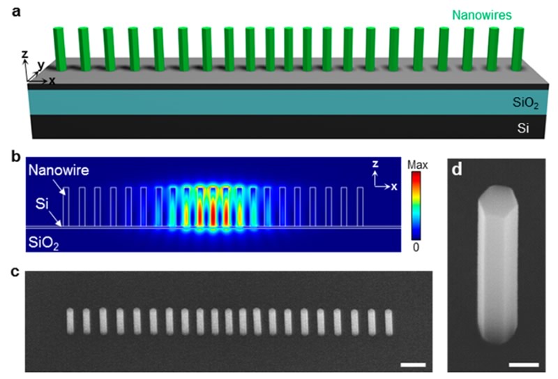
The applications of (nano)lasers are numerous and extremely varied. It is easy to find coherent light emitters in medicine, food science, manufacturing companies, military sector and research. III-V materials possess high gain value, direct band gap, and easy band gap tunability by varying the alloy component. The major problem of III-V materials growth on silicon is the lattice mismatch at the interface, which produces dislocation and poor performance. In III-V semiconductor nanowires (NWs) and nanopillars (NPs), the lattice mismatch can be fully relaxed over a small number of monolayers because of its small footprint. Moreover, NWs/NPs offer significant potential for nanoscale laser source due to the quasi-one-dimensional structure, which facilitates a natural Fabry-Perot resonator cavity and optical gain medium simultaneously.
In CAPPA, time-resolved photoluminescence (TRPL) measurements were performed on molecular-beam epitaxy (MBE) grown AlGaAs/GaAs nanolasers. The samples were excited using a Ti:Sapphire pulsed laser emitting 780 nm, 200fs pulses with a repetition rate of 80MHz. Streak images were recorded with the Hamamatsu streak camera. The photoluminescence peak was seen to red-shift over time because of carrier contrentation influence on material refractive index (Figs. 1 and 2).

Nano Letters, 17, 3465-3470, 2017
Molecular Imprinted Polymer
Molecularly imprinted Polymers (MIPs), first theorized in the mid-eighties are a synthetic molecular recognition tool that can be designed to specifically detect target molecules, macromolecules or even bacteria such as E. coli. MIPs are synthesized using cross polymerization techniques in conjunction with target molecules such that a specific target-polymer binding site is created. This binding site is sterically and chemically functionalized to bind to the unique target. In turn, molecular recognition and binding are highly specific to the target, even in a diverse chemical soup environment. MIPs share similar functionality to those of antibodies and enzymes, with the benefit that MIPs have the capability to become biomimetic sensors. MIPs compare very favourably to antibodies and enzymes, in that MIPs are cheaper to produce, more stable and more customizable. MIPs do not require tightly controlled environments that enzymes and antibodies mandate for stability and reactivity purposes. MIPs are further superior to enzymes and antibodies in their reusability, in that costly purification and salvage techniques are not required. The focus of this work is to couple MIPs with spectroscopic sensing techniques to provide low cost, real-time and portable detection of various hazardous molecules in a range of environments.


